- 您现在的位置:买卖IC网 > Sheet目录2003 > LTC1416IG#TR (Linear Technology)IC ADC 14BIT 400KSPS SMPL 28SSOP
3
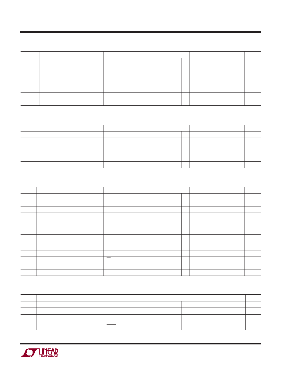
LTC1416
SYMBOL
PARAMETER
CONDITIONS
MIN
TYP
MAX
UNITS
S/(N + D)
Signal-to-(Noise + Distortion) Ratio
100kHz Input Signal
q
77
80.5
dB
200kHz Input Signal
80
dB
THD
Total Harmonic Distortion
100kHz Input Signal, First 5 Harmonics
q
–93
– 86
dB
200kHz Input Signal, First 5 Harmonics
– 90
dB
SFDR
Spurious-Free Dynamic Range
100kHz Input Signal
q
–95
– 86
dB
IMD
Intermodulation Distortion
fIN1 = 87.01172kHz, fIN2 = 113.18359kHz
– 90
dB
Full Power Bandwidth
15
MHz
Full Linear Bandwidth
S/(N + D)
≥ 77dB
0.8
MHz
SYMBOL
PARAMETER
CONDITIONS
MIN
TYP
MAX
UNITS
VIH
High Level Input Voltage
VDD = 5.25V
q
2.4
V
VIL
Low Level Input Voltage
VDD = 4.75V
q
0.8
V
IIN
Digital Input Current
VIN = 0V to VDD
q
±10
A
CIN
Digital Input Capacitance
5pF
VOH
High Level Output Voltage
VDD = 4.75V
IOUT = – 10A
4.5
V
IOUT = – 200A
q
4.0
V
VOL
Low Level Output Voltage
VDD = 4.75V
IOUT = 160A
0.05
V
IOUT = 1.6mA
q
0.10
0.4
V
IOZ
Hi-Z Output Leakage D13 to D0
VOUT = 0V to VDD, CS High
q
±10
A
COZ
Hi-Z Output Capacitance D13 to D0
CS High (Note 9 )
q
15
pF
ISOURCE
Output Source Current
VOUT = 0V
– 10
mA
ISINK
Output Sink Current
VOUT = VDD
10
mA
PARAMETER
CONDITIONS
MIN
TYP
MAX
UNITS
VREF Output Voltage
IOUT = 0
2.480
2.500
2.520
V
VREF Output Tempco
IOUT = 0
±15
ppm/
°C
VREF Line Regulation
4.75V
≤ VDD ≤ 5.25V
0.05
LSB/V
– 5.25V
≤ VSS ≤ –4.75V
0.05
LSB/V
VREF Output Resistance
– 0.1mA
≤ IOUT ≤ 0.1mA
4
k
COMP Output Voltage
IOUT = 0
4.06
V
The q denotes specifications which apply over the full operating temperature range,
otherwise specifications are at TA = 25°C. (Note 5)
DIGITAL I PUTS A D DIGITAL OUTPUTS
U
DY A IC ACCURACY
U
W
The q denotes specifications which apply over the full
operating temperature range, otherwise specifications are at TA = 25°C. (Note 5)
I TER AL REFERE CE CHARACTERISTICS
UU
U
The q denotes specifications which apply over the full
operating temperature range, otherwise specifications are at TA = 25°C. (Note 5)
SYMBOL
PARAMETER
CONDITIONS
MIN
TYP
MAX
UNITS
VDD
Positive Supply Voltage
(Note 10)
4.75
5.25
V
VSS
Negative Supply Voltage
(Note 10)
– 4.75
– 5.25
V
IDD
Positive Supply Current
q
710
mA
Nap Mode
SHDN = 0V, CS = 0V
1
1.6
mA
Sleep Mode
SHDN = 0V, CS = 5V
1
A
POWER REQUIRE E TS
W
U
The q denotes specifications which apply over the full operating temperature range,
otherwise specifications are at TA = 25°C. (Note 5)
发布紧急采购,3分钟左右您将得到回复。
相关PDF资料
LTC1417AIGN#TR
IC ADC 14BIT 400KSPS SMPL 16SSOP
LTC1418ACG#TRPBF
IC A/D CONV 14BIT SRL&PAR 28SSOP
LTC1419AISW#TRPBF
IC A/D CONV 14BIT SAMPLNG 28SOIC
LTC1420IGN#TRPBF
IC ADC 12BIT 10MSPS SAMPL 28SSOP
LTC1426IS8#TR
IC DAC PWM 6BIT DUAL MCPWR 8SOIC
LTC1427CS8-50#TRPBF
IC D/A CONV 10BIT W/SMBUS 8-SOIC
LTC1428CS8-50#TRPBF
IC D/A CONV 8BIT SINK OUT 8-SOIC
LTC1446LIS8#TRPBF
IC D/A CONV 12BIT R-R DUAL 8SOIC
相关代理商/技术参数
LTC1416IG#TRPBF
功能描述:IC A/D CONV 14BIT SAMPLNG 28SSOP RoHS:是 类别:集成电路 (IC) >> 数据采集 - 模数转换器 系列:- 标准包装:1,000 系列:- 位数:16 采样率(每秒):45k 数据接口:串行 转换器数目:2 功率耗散(最大):315mW 电压电源:模拟和数字 工作温度:0°C ~ 70°C 安装类型:表面贴装 封装/外壳:28-SOIC(0.295",7.50mm 宽) 供应商设备封装:28-SOIC W 包装:带卷 (TR) 输入数目和类型:2 个单端,单极
LTC1417ACGN
功能描述:IC A/D CONV 14BIT SAMPLNG 16SSOP RoHS:否 类别:集成电路 (IC) >> 数据采集 - 模数转换器 系列:- 标准包装:1,000 系列:- 位数:12 采样率(每秒):300k 数据接口:并联 转换器数目:1 功率耗散(最大):75mW 电压电源:单电源 工作温度:0°C ~ 70°C 安装类型:表面贴装 封装/外壳:24-SOIC(0.295",7.50mm 宽) 供应商设备封装:24-SOIC 包装:带卷 (TR) 输入数目和类型:1 个单端,单极;1 个单端,双极
LTC1417ACGN#PBF
功能描述:IC A/D CONV 14BIT SAMPLNG 16SSOP RoHS:是 类别:集成电路 (IC) >> 数据采集 - 模数转换器 系列:- 标准包装:1 系列:microPOWER™ 位数:8 采样率(每秒):1M 数据接口:串行,SPI? 转换器数目:1 功率耗散(最大):- 电压电源:模拟和数字 工作温度:-40°C ~ 125°C 安装类型:表面贴装 封装/外壳:24-VFQFN 裸露焊盘 供应商设备封装:24-VQFN 裸露焊盘(4x4) 包装:Digi-Reel® 输入数目和类型:8 个单端,单极 产品目录页面:892 (CN2011-ZH PDF) 其它名称:296-25851-6
LTC1417ACGN#TR
功能描述:IC ADC 14BIT 400KSPS SMPL 16SSOP RoHS:否 类别:集成电路 (IC) >> 数据采集 - 模数转换器 系列:- 标准包装:1,000 系列:- 位数:12 采样率(每秒):300k 数据接口:并联 转换器数目:1 功率耗散(最大):75mW 电压电源:单电源 工作温度:0°C ~ 70°C 安装类型:表面贴装 封装/外壳:24-SOIC(0.295",7.50mm 宽) 供应商设备封装:24-SOIC 包装:带卷 (TR) 输入数目和类型:1 个单端,单极;1 个单端,双极
LTC1417ACGN#TRPBF
功能描述:IC A/D CONV 14BIT SAMPLNG 16SSOP RoHS:是 类别:集成电路 (IC) >> 数据采集 - 模数转换器 系列:- 标准包装:1,000 系列:- 位数:12 采样率(每秒):300k 数据接口:并联 转换器数目:1 功率耗散(最大):75mW 电压电源:单电源 工作温度:0°C ~ 70°C 安装类型:表面贴装 封装/外壳:24-SOIC(0.295",7.50mm 宽) 供应商设备封装:24-SOIC 包装:带卷 (TR) 输入数目和类型:1 个单端,单极;1 个单端,双极
LTC1417AIGN
功能描述:IC A/D CONV 14BIT SAMPLNG 16SSOP RoHS:否 类别:集成电路 (IC) >> 数据采集 - 模数转换器 系列:- 标准包装:1,000 系列:- 位数:12 采样率(每秒):300k 数据接口:并联 转换器数目:1 功率耗散(最大):75mW 电压电源:单电源 工作温度:0°C ~ 70°C 安装类型:表面贴装 封装/外壳:24-SOIC(0.295",7.50mm 宽) 供应商设备封装:24-SOIC 包装:带卷 (TR) 输入数目和类型:1 个单端,单极;1 个单端,双极
LTC1417AIGN#PBF
功能描述:IC A/D CONV 14BIT SAMPLNG 16SSOP RoHS:是 类别:集成电路 (IC) >> 数据采集 - 模数转换器 系列:- 其它有关文件:TSA1204 View All Specifications 标准包装:1 系列:- 位数:12 采样率(每秒):20M 数据接口:并联 转换器数目:2 功率耗散(最大):155mW 电压电源:模拟和数字 工作温度:-40°C ~ 85°C 安装类型:表面贴装 封装/外壳:48-TQFP 供应商设备封装:48-TQFP(7x7) 包装:Digi-Reel® 输入数目和类型:4 个单端,单极;2 个差分,单极 产品目录页面:1156 (CN2011-ZH PDF) 其它名称:497-5435-6
LTC1417AIGN#TR
功能描述:IC ADC 14BIT 400KSPS SMPL 16SSOP RoHS:否 类别:集成电路 (IC) >> 数据采集 - 模数转换器 系列:- 标准包装:1,000 系列:- 位数:12 采样率(每秒):300k 数据接口:并联 转换器数目:1 功率耗散(最大):75mW 电压电源:单电源 工作温度:0°C ~ 70°C 安装类型:表面贴装 封装/外壳:24-SOIC(0.295",7.50mm 宽) 供应商设备封装:24-SOIC 包装:带卷 (TR) 输入数目和类型:1 个单端,单极;1 个单端,双极